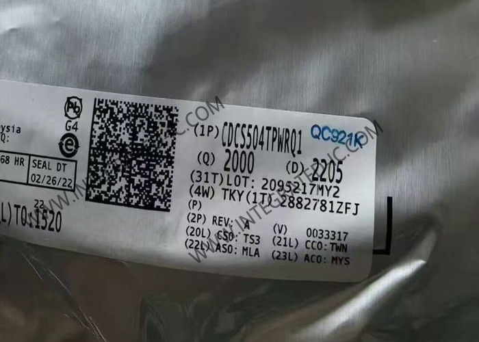
CDCS504TPWRQ1 Integrated Circuit Chip LVCMOS Input Clock Buffer With Selectable Frequency Multiplication
Product Description Of CDCS504TPWRQ1
CDCS504TPWRQ1 device is a LVCMOS input clock buffer with selectable frequency multiplication.
CDCS504TPWRQ1 has an output enable pin.
The device accepts a 3.3-V LVCMOS signal at the input.
The input signal is processed by a phased-locked loop (PLL), whose output frequency is either equal to the input frequency or multiplied by the factor of four.
By this, the device can generate output frequencies between 2 MHz and 108 MHz.
A separate control pin can be used to enable or disable the output. The CDCS504TPWRQ1 device operates in a 3.3-V environment.
It is characterized for operation from –40°C to 105°C and is available in an 8-pin TSSOP package.
Product Attributes Of CDCS504TPWRQ1
|
Type
|
|
|
Number of Circuits
|
|
|
Ratio - Input:Output
|
|
|
Differential - Input:Output
|
|
|
Input
|
|
|
Output
|
|
|
Frequency - Max
|
|
|
Voltage - Supply
|
|
|
Operating Temperature
|
|
|
Mounting Type
|
|
|
Grade
|
|
Feature Of CDCS504TPWRQ1
Qualified for Automotive Applications
AEC-Q100 Test Guidance With the Following Results:
Device Temperature Grade 2: –40°C to 105°C Ambient Operating Temperature Range
Device HBM ESD Classification Level H2
Device CDM ESD Classification Level C3B
Part of a Family of Easy-to-Use Clock Generator Devices
Clock Multiplier With Selectable Output Frequency
Frequency Multiplication Selectable Between x1 or x4 With One External Control Pin
Output Disable Through Control Pin
Single 3.3-V Device Power Supply
Wide Temperature Range: –40°C to 105°C
Low Space Consumption 8-Pin TSSOP Package
Create a Custom Design Using the CDCS504-Q1 With the WEBENCH® Power Designer
Applications Of CDCS504TPWRQ1
Automotive Applications Requiring Clock Multiplication
Other Electronic Components In Stock
|
Part Number
|
Package
|
|
R7FA4M3AD2CBM
|
144-LFBGA
|
|
R7FA6M2AD3CFP
|
100-LFQFP
|
|
R7FA6M2AD3CFB
|
144-LFQFP
|
|
R7FA6M3AF3CFP
|
100-LFQFP
|
|
R7FA6T2AD3CFL
|
48-LFQFP
|
|
R7FS1JA783A01CNE
|
48-WFQFN
|
|
R7FS3A17C3A01CFM
|
64-LFQFP
|
|
R7FA6T2AB3CNB
|
64-WFQFN
|
|
LIFCL-40-7BG256A
|
256-CABGA
|
|
LIFCL-40-7MG121A
|
121-CSFBGA
|
|
LIFCL-17-7BG256A
|
256-CABGA
|
|
LIFCL-17-7MG121A
|
121-CSFBGA
|
|
LIFCL-40-9BG400I
|
400-CABGA
|
|
LIFCL-40-8BG400I
|
400-CABGA
|
|
LIFCL-40-9BG256I
|
BGA-256
|
|
LIFCL-40-8BG256I
|
256-CABGA
|
|
LIFCL-40-9MG289I
|
289-CSBGA
|
|
LIFCL-40-8MG289I
|
289-CSBGA
|
|
LIFCL-40-7MG289I
|
289-CSBGA
|
|
LIFCL-40-9MG121I
|
121-CSFBGA
|
|
LIFCL-40-8MG121I
|
121-CSFBGA
|
|
LIFCL-40-7MG121I
|
121-CSFBGA
|
|
LIFCL-40-9SG72I
|
72-QFN
|
|
LIFCL-40-8SG72I
|
72-QFN
|
|
LIFCL-40-7SG72I
|
72-QFN
|
|
LIFCL-17-9BG256I
|
256-CABGA
|
|
LIFCL-17-8BG256I
|
256-CABGA
|
|
LIFCL-17-9MG121I
|
121-CSFBGA
|
|
LIFCL-17-8MG121I
|
121-CSFBGA
|
|
LIFCL-17-9SG72I
|
72-QFN
|
FAQ
Q: Are your products original?
A: Yes, all products are original, new original import is our purpose.
Q:Which Certificates do you have?
A:We are ISO 9001:2015 Certified Company and member of ERAI.
Q:Can you support small quantity order or sample?Is the sample free?
A:Yes,we support sample order and small order.Sample cost is different according to your order or project.
Q:How to ship my order? Is it safe?
A:We use express to ship,such as DHL,Fedex,UPS,TNT,EMS.We can also use your suggested forwarder.Products will be in good packing and ensure the safety and we are responsible to product damage to your order.
Q:What about the lead time?
A:We can ship stock parts within 5 working days.If without stock,we will confirm lead time for you based on your order quantity.

 Your message must be between 20-3,000 characters!
 English