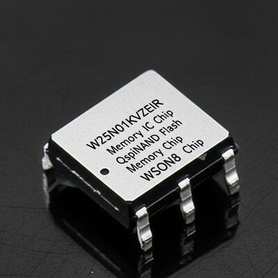
W25N01KVZEIR Memory IC Chip - 1Gbit SLC QspiNAND Flash Memory
The W25N01KVZEIR is a 1Gbit SLC QspiNAND Flash Memory IC that provides an optimal storage solution for systems with limited space, pin count, and power requirements. This advanced memory chip operates on a single 2.7V to 3.6V power supply with remarkably low current consumption of just 25mA during active operation and 10µA in standby mode.
The 1Gbit memory array is organized into 65,536 programmable pages, each containing 2,048 bytes. Complete pages can be programmed simultaneously using data from the internal 2,048-byte buffer, while erasure operations are performed in groups of 64 pages (128KB block erase).
Technical Specifications
| Parameter |
Specification |
| Series |
SpiFlash® |
| Memory Type |
Non-Volatile |
| Memory Format |
FLASH |
| Technology |
FLASH - NAND (SLC) |
| Memory Size |
1Gbit |
| Memory Organization |
128M x 8 |
| Memory Interface |
SPI - Quad I/O |
| Clock Frequency |
104 MHz |
| Write Cycle Time |
700µs |
| Access Time |
7 ns |
| Voltage Supply |
2.7V ~ 3.6V |
| Operating Temperature |
-40°C ~ 85°C (TA) |
| Mounting Type |
Surface Mount |
| Package / Case |
8-WDFN Exposed Pad |
| Supplier Device Package |
8-WSON (8x6) |
Key Features
QspiNAND Memory Family
- W25N01KV: 1G-bit / 128M-Byte capacity
- Standard SPI interface with CLK, /CS, DI, DO, /WP, /Hold
- Dual SPI support with CLK, /CS, IO0, IO1, /WP, /Hold
- Quad SPI interface with CLK, /CS, IO0, IO1, IO2, IO3
- Compatible with standard SPI serial flash commands
High Performance Operation
- 104MHz Standard/Dual/Quad SPI clock speeds
- 208/416MHz equivalent Dual/Quad SPI performance
- Fast program and erase operations
- 60,000 erase/program cycles endurance
- 10-year data retention capability
Power Efficiency & Reliability
- Single 2.7V to 3.6V power supply
- Low power consumption: 25mA active, 10µA standby
- Wide operating temperature range: -40°C to +85°C/105°C
Advanced Architecture
- Flexible 128KB block erase architecture
- Uniform 128K-Byte block erase capability
- Multiple page data load methods for enhanced flexibility
Enhanced Security & Protection
- On-chip 4-Bit ECC for memory array integrity
- Blocks 0-7 and 1020-1023 factory-validated with ECC enabled
- ECC status bits for result monitoring
- Software and hardware write-protection
- Power supply lock-down and OTP protection
- Unique ID and parameter pages
- Ten 2KB OTP pages for secure data storage
Related Electronic Components
| Part Number |
Package |
| AGFB023R31C3E3V |
3184-FBGA |
| AGFD019R31C3E4X |
3184-FBGA |
| AGFD019R31C2I1V |
3184-FBGA |
| AGFD019R24C2E2VB |
2340-BGA |
| AGFD019R24C2E3E |
2340-BGA |
| AGFD019R24C2E4X |
2340-BGA |
| AGIB019R18A2I3E |
1805-FBGA |
| AGIB022R31A2I1VB |
3184-FBGA |
| AGFB023R25A2E3E |
2581-FBGA |
| AGFB022R24C2I3E |
BGA |
Frequently Asked Questions
Are your products original?
Yes, all products are original. Sourcing new original imported components is our primary business focus.
Which Certificates do you have?
We are an ISO 9001:2015 Certified Company and an active member of ERAI.
Can you support small quantity orders or samples? Is the sample free?
Yes, we support sample orders and small quantity purchases. Sample costs vary depending on your specific order requirements and project scope.
How do you ship my order? Is it safe?
We utilize major express carriers including DHL, FedEx, UPS, TNT, and EMS. We can also accommodate your preferred shipping forwarder. All products are carefully packaged to ensure safety during transit, and we assume responsibility for any damage to your order.
What is the lead time?
Stock parts are typically shipped within 5 working days. For non-stock items, we will confirm the lead time based on your specific order quantity.

 Your message must be between 20-3,000 characters!
 English